ADC
- Thomas Watteyne
This section refers to the following sample application(s):
02-adc
The LTC5800
The voltage applied to the ADC input pins must be between 0V and +1.8V. Applying a voltage outside that range will damage the part.
Two internal channels are also available to sample supply voltage and temperature. These are discussed in the following sections:
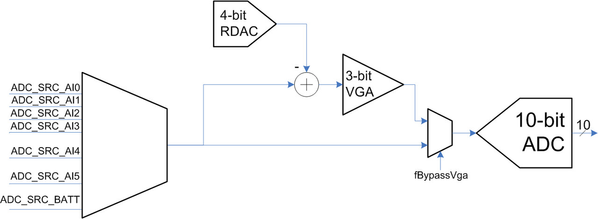
ADC samples are configured, initiated, and read manually; periodic or triggered-input sampling is not supported. The analog channel has several configurable parameters that determine its behavior.
Analog Inputs
The following table lists the external input channels and the corresponding labels on the on the silkscreen of the
board:| Input | On-Chip Software Development Kit | |
|---|---|---|
| Analog input 0 | DN_ADC_AI_0_DEV_ID | AI_0 |
| Analog input 1 | DN_ADC_AI_1_DEV_ID | AI_1 |
| Analog input 2 | DN_ADC_AI_2_DEV_ID | AI_2 |
| Analog input 3 | DN_ADC_AI_3_DEV_ID | AI_3 |
RDAC and VGA
The analog channel on
LTC5800
can be configured to provide accurate measurements of an analog input signal. The ADC itself has a scale from 0V to 1.8V, with a 10-bit resolution. Each LSB represents 1.8mV.The Variable-Gain Amplifier (VGA) and offset Range-DAC (RDAC) provide improved resolution of analog input signals having less than full-scale input swing. Improved resolution is attained by zooming into a user-configured portion of the full 0 to 1.8V input range. To zoom into the desired input-voltage range, the RDAC value is first subtracted from the analog input signal; the result of this subtraction is then amplified by the VGA by a user-settable gain from 1 to 8. Zooming to the range of interest in this fashion allows the dynamic range of the ADC to be matched to the input signal to be digitized.
The RDAC is 4-bits and has sixteen equally-spaced, discrete offset ranges as follows:
On-Chip Software Development Kit | Nominal Center of Analog Input Range (mV) |
|---|---|
DN_ADC_RDAC_113mV | 113 |
DN_ADC_RDAC_225mV | 225 |
DN_ADC_RDAC_338mV | 338 |
DN_ADC_RDAC_450mV | 450 |
DN_ADC_RDAC_563mV | 563 |
DN_ADC_RDAC_675mV | 675 |
DN_ADC_RDAC_788mV | 788 |
DN_ADC_RDAC_900mV | 900 |
DN_ADC_RDAC_1013mV | 1013 |
DN_ADC_RDAC_1125mV | 1125 |
DN_ADC_RDAC_1238mV | 1238 |
DN_ADC_RDAC_1350mV | 1350 |
DN_ADC_RDAC_1463mV | 1463 |
DN_ADC_RDAC_1575mV | 1575 |
DN_ADC_RDAC_1688mV | 1688 |
DN_ADC_RDAC_1800mV | 1800 |
The VGA has eight discrete gain settings as follows:
On-Chip Software Development Kit | VGA Gain | Nominal Full-Scale Input Swing (mVpp) |
|---|---|---|
DN_ADC_VGA_1800mVpp | 1 | 1800 |
DN_ADC_VGA_900mVpp | 2 | 900 |
DN_ADC_VGA_600mVpp | 3 | 600 |
DN_ADC_VGA_450mVpp | 4 | 450 |
DN_ADC_VGA_360mVpp | 5 | 360 |
DN_ADC_VGA_300mVpp | 6 | 300 |
DN_ADC_VGA_257mVpp | 7 | 257 |
DN_ADC_VGA_225mVpp | 8 | 225 |
Example Use Case
Problem: Use the VGA and RDAC to sample a humidity sensor circuit having an output swing from 500mV (0% RH) to 900mV (100% RH).
Solution: The middle of the sensor output swing is 700mV. The closest RDAC setting is RDAC = 5 which corresponds to a 675mV offset. To handle the full sensor input swing we choose a gain of 3 which provides an input dynamic range of 600mV (+/-300mV) around 675mV. Thus choosing an RDAC setting of 5 and a gain of 3 zooms the range of the analog input to 375mV to 975mV.
If the input signal extends beyond the selected range of interest, the device will return an incorrect value. If it is possible that the analog input signal will exceed the selected range of interest, a preliminary low-gain conversion should be made to allow proper configuration of the RDAC and gain settings.
The 02-adc Sample Application
The 02-adc sample application periodically reads the voltage on analog input 0. This results in the following CLI output when connecting a bench power supply (set to out 1.0V) to the AI_0 pin:
adc app, ver 1.0.0.1
SmartMeshIP stack, ver 1.2.1.3
adcVal=10002
adcVal=9984
adcVal=9984
adcVal=9984
adcVal=10002
adcVal=10002
adcVal=9984
adcVal=9984
The sample application prints the raw values returned by the DN_ADC_AI_0_DEV_ID device, which is expressed in tenths of mV.
Refer to the
SmartMesh On-Chip API html documentation
in the /doc directory of the for documentation about this feature.